Jerry Woodall
Bio – Experience – Top 20 Pubs – Memberships – Awards
Contact
Office: 2001 Kemper Hall
Phone (office): 530-752-9581
Email: jwoodall@ucdavis.edu
Degrees
- Ph.D. in Electrical Engineering (1982), Cornell University
- Thesis: Gallium Arsenide MESFET Technology: Ion Implantation and Metal Contact
- B.S. in Metallurgy (1960), Massachusetts Institute of Technology
Biography
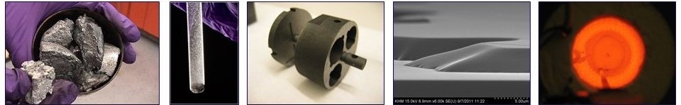
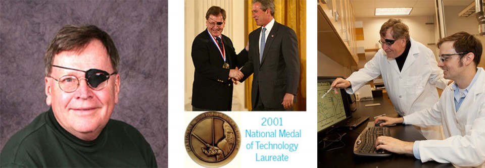
Jerry M. Woodall, a National Medal of Technology Laureate, and Distinguished Professor of Electrical and Computer Engineering at UC Davis, received a B.S. in metallurgy in 1960 from MIT. In 1982, he was awarded a Ph.D. in Electrical Engineering from Cornell University. He pioneered and patented the development of GaAs high efficiency IR LEDs, used today in remote control and data link applications such as TV sets and IR LAN. This was followed by the invention and seminal work on gallium aluminum arsenide (GaAlAs) and GaAlAs/GaAs heterojunctions used in super-bright red LEDs and lasers used, for example, in CD players and short link optical fiber communications. He also pioneered and patented the GaAlAs/GaAs heterojunction bipolar transistor used in, for example, cellular phones. Also, using GaAs/InGaAs strained, non-lattice-matched heterostructures, he pioneered the “pseudomorphic” high electron mobility transistor (HEMT), a state-of-the-art high speed device widely used in cellular phones. The technological and commercial importance of his seminal work led to the 2000 Nobel Prize in Physics for heterojunctions awarded to Herbert Kroemer and Zhores Alferov. His demonstration of the GaAlAs/GaAs heterojunction led to the creation of important new areas of solid-state physics, such as: superlattice, low dimension, mesoscopic, and resonant tunneling physics. Also, using the technique called molecular beam epitaxy (MBE) and the GaAs/InGaAs strained, non-lattice-matched heterostructure, he pioneered the “pseudomorphic” high electron mobility transistor (HEMT), a state-of-the-art high speed device widely used in devices and circuits including those found in cellular phones. This work led to the use of the pseudomorphic InAs/GaAs heterostructure to make “self-organized” quantum dots, a currently popular topic in physics. His recent past work involves the MBE growth of III-V materials and devices with special emphasis on metal contacts, the thermodynamics of extremely large doping concentrations, and devices made of non-lattice matched heterojunctions and substrates. More recently he invented, developed and published a breakthrough global scale “green” energy storage technology in which bulk aluminum rich alloys split both fresh water and salt water into hydrogen gas on demand, thus obviating the need to store and transport hydrogen. The aluminum hydroxide reaction product is easily recycled back to aluminum via the commercial Hall electrolysis process. This feature coupled with the fact that aluminum has the highest volumetric total chemical energy density known, and the fact that aluminum has the highest volumetric total chemical energy density known, and the fact that aluminum is the third most abundant element on earth’s surface promises to make this technology a serious contender for a long haul, global scale, economically viable, alternative green energy solution.
His efforts are recorded in over 350 publications in the open literature, and 85 issued U.S. patents. His accomplishments have been recognized by his election as IBM Fellow in 1985, an $80,000 IBM Corporate Award in 1992 for the invention of the GaAlAs/GaAs heterojunction, and the 2001 National Medal of Technology awarded by the President of the United States.
Other recognition includes the 1980 Electronics Division Award of the Electrochemical Society (ECS), the 1984 IEEE Jack A. Morton Award, the 1985 ECS Solid State Science and Technology Award, the 1988 Heinrich Welker Gold Medal and International GaAs Symposium Award, the 1990 American Vacuum Society (AVS) Medard Welch (Founder’s) Award, its highest honor, the 1997 Eta Kappa Nu Vladimir Karapetoff Eminent Members’ Award, the 1998 American Society for Engineering Education’s General Electric Senior Research Award, the 1998 Electrochemical Society’s (ECS) Edward Goodrich Acheson (Founder’s) Award, its highest honor, ECS Honorary Member (2009), an IEEE Third Millennium Medal (2000), the Federation of Materials Societies’ 2002 National Materials Advancement Award, and the 2005 IEEE Jun-ichci Nishizawa Gold Medal. Honorific recognition includes his election to the National Academy of Engineering in 1989, Fellow of the American Physical Society in 1982, IEEE Fellow in 1990, ECS Fellow in 1992, and AVS Fellow in 1994. His national professional society activities include President of the ECS (1990), and President of AVS (1998).
Professional Experience
- 2012-present: Distinguished Professor of ECE, University of California, Davis, CA
- 2008-2012: Barry and Patricia Epstein Distinguished Professor of ECE, Purdue University, West Lafayette, IN and National Medal of Technology Laureate
- 2005-2008: Purdue University Distinguished Professor of ECE, Purdue University, West Lafayette, IN and National Medal of Technology Laureate
- 1999-2004: C. Baldwin Sawyer Professor of Electrical Engineering and National Medal of Technology Laureate, Yale University, New Haven, CT
- 1993-1998: Charles William Harrison Distinguished Professor of Microelectronics, Purdue University, West Lafayette, IN
- 1985-1993: IBM Corporate Fellow, IBM Research, Yorktown Hts, NY
- 1962-1985: Research Staff Member, IBM Research, Yorktown Hts, NY
- 1960-1962: Staff Engineer, Clevite Transistor Products, Waltham, MA
Top 20 Journal Publications
- H. Rupprecht, J. M. Woodall, K. Konnerth, and D. G. Pettit, “Efficient Electroluminescence from GaAs Diodes at 300°K” Applied Physics Letters, vol. 9, pp. 221-223, 1966. [pdf] Opens in a new window doi: 10.1063/1.1754721
- This was the first report of a high-efficiency LED, the first fabrication of an LED by the liquid phase epitaxy (LPE) method, and the first use of Si as both an n-type and p-type dopant. To date, this LED remains the LED of choice for IR signal, control, and IR LAN. It is covered by a U.S. patent.
- H. Rupprecht, J. M. Woodall, and G. D. Pettit, “Efficient Visible Electroluminescence at 300°K from Ga1-xAlxAs p-n Junctions Grown by Liquid-Phase Epitaxy” Applied Physics Letters, vol. 11, pp. 81-83, 1967. [pdf] Opens in a new window doi: 10.1063/1.1754721
- The first useful demonstration of the lattice-matched heterojunction, this publication opened the field of heterojunction research in general. It is covered by a U.S patent.
- J. M. Woodall and H. J. Hovel, “High Efficiency Ga1-xAlxAs – GaAs Solar Cells” Applied Physics Letters, vol. 21, pp. 379-381, 1972. [pdf] Opens in a new window doi: 10.1063/1.1654421
- This seminal publication demonstrated the use of GaAlAs/GaAs for high-efficiency solar cells and showed that this heterojunction greatly reduced surface recombination in GaAs. It is covered by U.S. patents.
- W. P. Dumke, J. M. Woodall and V. L. Rideout, “GaAs-GaAlAs Heterojunction Transistor for High Frequency Operation” Solid-State Electronics, vol. 15, pp. 1339-1343, 1972. [pdf] Opens in a new window doi: 10.1016/0038-1101(72)90127-X
- This research marked the first realization of HBTs and forms the basis of the power amplifier stage of current cellular phones. It is covered by a U.S. patent.
- J. Rosenberg, M. Benlarmi, P. D. Kirchner, J. M. Woodall and G. D. Pettit, “An In0.15Ga0.85As/GaAs Pseudomorphic Single Quantum Well HEMT” IEEE Electron Device Letters, vol. 6, pp. 491-493, 1985. [pdf] Opens in a new window doi: 10.1109/EDL.1985.26205
- This paper describes what continues to be the device of choice for low-noise small-signal amplification in many applications, including cellular phones.
- D. L. Rogers, J. M. Woodall, G. D. Pettit and D. McInturff, “High Performance, 1.3 Micron, GaInAs Detectors Fabricated on GaAs Substrates” IEEE Electron Device Letters, vol. 9, pp. 515-517, 1988.[pdf] Opens in a new window doi: 10.1109/55.17829
- This is the first demonstration of an enabler to allow the integration of InGaAs 1.3-1.5 photonic devices with GaAs high-speed electronic circuits.
- J. M. Woodall, J. Freeouf, G. D. Pettit, T. N. Jackson, and P. D. Kirchner, “Ohmic Contacts to n-GaAs Using Graded Band Gap Layers of Ga1-xInxAs Grown by Molecular Beam Epitaxy” J. of Vacuum Science and Technology, vol. 19, pp. 626-627, 1981. [pdf] Opens in a new window doi: 10.1116/1.571074
- This is a state-of-the-art ohmic contact widely used by companies that fabricate HBTs for applications that include cellular phones.
- P. E. Dodd, M. L. Lovejoy, M. S. Lundstrom, M. R. Melloch, J. M. Woodall and J. D. Pettit, “Demonstration of npn InAs Bipolar Transistors with Inverted Base Doping” IEEE Electron Device Letters, vol. 17, pp. 166-168, 1996. [pdf] Opens in a new window doi: 10.1109/55.485162
- This is the first reported demonstration of an InAs-based bipolar transistor. It is important because it offers the possibility of terahertz frequency performance.
- S. Tiwari, G. D. Pettit, R. J. Davis, and J. M. Woodall, “High Efficiency and Low Threshold Current Strained V-Groove Quantum-Wire Lasers” Applied Physics Letters, vol. 64, pp. 3536-3538, 1994.[pdf] Opens in a new window doi: 10.1063/1.111264
- This was the first demonstration of an injection lase with threshold currents well below 1 mA, opening the possibility for realistic optical interconnects for high-density integrated electronic circuits.
- R. C. Gee, T. P. Chin, C. W. Tu, P. M. Asbeck, C. L. Lin, P. D. Kirchner and J. M. Woodall, “InP/InGaAs HBTs Grown by GSMBE with Carbon Doped Base” IEEE Electron Device Letters, vol. 13, pp. 247-249, 1992. [pdf] Opens in a new window doi: 10.1109/55.145042
- This HBT device is thought to be a strong candidate for the next-generation technology for cellular phones. It was demonstrated through a manufacturing technology of choice.
- J. J. Cuomo, J. F. Ziegler and J. M. Woodall, “A New Concept for Solar Energy Thermal Conversion” Applied Physics Letters, vol. 26, pp. 557-559, 1975. [pdf]Opens in a new window doi: 10.1063/1.87990
- This was a revolutionary way to efficiently convert solar energy into heat.
- S. D. Offsey, J. M. Woodall, A. C. Warren, P. D. Kirchner, T. C. Chappell and G. D. Pettit, “Unpinned (100) GaAs Surfaces in Air Using Photochemistry” Applied Physics Letters, vol. 48, pp. 475-477, 1986. [pdf] Opens in a new window doi: 10.1063/1.96535
- This was a seminal demonstration that the problem of Fermi-level pinning at GaAs surfaces could be eliminated and, hence, was not due to a fundamental physical limitation. This opened the way to the subsequent demonstration of a GaAs MOS technology and new surface passivation techniques.
- J. Freeouf and J. M. Woodall, “Schottky Barriers: An Effective Workfunction Model” Applied Physics Letters, vol. 39, pp. 727-729, 1981. [pdf] Opens in a new window doi: 10.1063/1.92863
- This paper provided a new way of understanding Fermi-level pinning at compound semiconductor surfaces. Its technological implications led to, e.g., the results of paper 12 above.
- J. M. Woodall, G. D. Pettit, T. N. Jackson, C. Lanza, K. Kavanaugh, and J. Meyer, “Fermi-Level Pinning by Misfit Dislocations at GaAs Interfaces” Physical Review Letters, vol. 51, pp. 1783-1786, 1983. [pdf] Opens in a new window doi: 10.1103/PhysRevLett.51.1783
- This is a fundamental interface physics study demonstrating a new mechanism for Fermi-level pinning at lattice mismatched interfaces.
- J. C. P. Chang, T. P. Chin and J. M. Woodall, “Incoherent Interface of InAs Grown Directly on GaP(100)” Applied Physics Letters, vol. 69, pp. 981-983, 1996. [pdf] Opens in a new window doi: 10.1063/1.117102
- This is a seminal paper showing that good-quality epilayers of InAs can be grown on GaP substrates. This is a revolutionary result, as it was widely believed that high-quality epilayers of materials with a large lattice constant mismatch relative to the substrate could not be successfully grown. (InAs/GaP has an 11% lattice mismatch.)
- M. D. Pashley, K. W. Haberern, W. Friday, J. M. Woodall, and P. D. Kirchner, “The Structure of GaAs (001) (2×4)-c(2×8) Determined by Scanning Tunneling Microscopy” Physical Review Letters, vol. 60, pp. 2176-2179, 1988. [pdf] Opens in a new windowdoi: 10.1103/PhysRevLett.60.2176
- The very first report of scanning tunneling microscopy of MBE-grown GaAs surfaces, this paper was cited at the plenary session of the International Conference of the Physics of Semiconductors, 1988, Warsaw, Poland. It was the first experimental proof of current theories for the atomic structure of GaAs surfaces.
- L. J. Brillson, M. L. Slade, R. E. Viturro, M. K. Kelly, N. Tache, G. Margaritondo, J. M. Woodall, P. D. Kirchner, G. D. Pettit, and S. L. Wright, “Absence of Fermi-Level Pinning at Metal-InxGa1-xAs(100) Interfaces” Applied Physics Letters, vol. 48, pp. 1458-1460, 1986. [pdf] Opens in a new window doi: 10.1063/1.97027
- A seminal paper that demonstrates Schottky limit behavior (no Fermi-level pinning) for MBE-grown GaInAs and low-temperature deposition of metals. It also demonstrates the validity of paper 13 above.
- J. M. Woodall, “Solution Grown Ga1-xAlxAs Superlattice Structures” J. Crystal Growth, vol. 12, pp. 32-38, 1972. [pdf] Opens in a new window doi: 10.1016/0022-0248(72)90334-X
- The first report of fabricating superlattice structures using GaAlAs/GaAs materials. The invention of the semiconductor superlattice and its physics on GaAlAs/GaAs has led to many prizes and awards.
- R. M. Feenstra, J. M. Woodall, and G. D. Pettit, “Observation of Bulk Defects by Scanning Tunneling Microscopy and Spectroscopy: Arsenic Antisite Defects in GaAs” Physical Review Letters, vol. 71, pp. 1176-1179, 1993. [pdf] Opens in a new window doi: 10.1103/PhysRevLett.71.1176
- This paper is the seminal work on the electronic properties of As-related defects described in paper #20 below.
- C. Warren, J. M. Woodall, J. L. Freeouf, D. Grischkowsky, D. T. McInturff, M. R. Melloch, and N. Otsuka, “Arsenic Precipitates and the Semi-Insulating Properties of GaAs Buffer Layers Grown by Low Temperature Molecular Beam Epitaxy” Applied Physics Letters, vol. 57, pp. 1331-1333, 1990.[pdf] Opens in a new windowdoi: 10.1063/1.103474
- This is the first report of the properties of As precipitates in GaAs grown by MBE at low substrate temperatures. Since this publication, the authors have demonstrated many important applications including launching a company that has commercialized a state-of-the-art, high-speed photodetector. This breakthrough is covered by a U.S. patent.
Honorary Society Memberships
- Honorary Member – The Electrochemical Society (ECS), 2007 (only 76 out of 15,000 members have held this rank since the society’s inception in 1919, including Thomas Edison)
- Fellow – American Vacuum Society (AVS), 1994
- Fellow – The Electrochemical Society (ECS), 1992
- Fellow – Institute of Electrical and Electronics Engineers (IEEE), 1990
- Member – National Academy of Engineering (NAE), 1989
- Fellow – American Physical Society (APS), 1982
Honors and Awards
- 2005 IEEE Jun-ichci Nishizawa Medal “For pioneering contributions to the LPE in the GaAs/AlGaAs systems, including applications to photonic and electronic devices”
- 2002 The Federation of Materials Societies (FMS) National Materials Advancement Award
- 2001 National Medal of Technology (a U.S. Presidential Award presented in 2002)
- 2000 IEEE Electron Devices Society (EDS) Millennium Medal
- 1998 The Electrochemical Socienty (ECS) Edward Goodrich Acheson Award
- 1998 ASEE General Electric Senior Research Award
- 1997-1998 Eta Kappa Nu Vladamir Karapetoff Outstanding Technical Achievement Award
- 1990 American Vacuum Society Medard W. Welch Award
- 1988 Gallium Arsenide Symposium Award and Heinrich Welker Gold Medal
- 1985 The Electrochemical Society Solid State Science and Technology Award
- 1984 IEEE Jack A. Morton Award
- 1980 The Electrochemical Society Electronics Division Award
- 1975 Industrial Research IR-100 Award for “Dendritic Solar Energy Conversion Surface”
- Nine NASA Certificates of Recognition Awards
- 1992-IBM Corporate Award of $80,000 for inventing the GaAlAs/GaAs heterojunction
- 1989-IBM Outstanding Innovation Award for Pioneering Work in Heterojunction Bipolar Transistors
- 1979-IBM Outstanding Innovation Award for Improved GaAlAs/GaAs Solar Cells
- 1972-IBM Outstanding Invention Award for GaAlAs/GaAs High Efficiency Solar Cells
- 1970-IBM Outstanding Contribution Award for High Efficiency GaAs and GaAlAs Light Emitting Diodes
- 1967-IBM Outstanding Invention Award for a Process for Preparing High Purity Low Resistivity GaAs Crystals
- 1967-1992-Thirty IBM Invention Achievement Awards